
Introduction
Material outgassing semiconductor vacuum is a key consideration for wafer processing hardware. In semiconductor wafer manufacturing, vacuum cleanliness directly impacts process yield. Even trace gas release, known as material outgassing, from internal chamber hardware can release volatile condensable contaminants, trigger plasma instability, generate micro-particles and ruin delicate thin-film processes including PVD, CVD, plasma etching and atomic layer deposition (ALD).
Outgassing refers to volatile molecules and gases desorbing from solid surfaces or diffusing out of bulk material under high vacuum or ultra-high vacuum (UHV). Semiconductor vacuum hardware designers rely on two core evaluation metrics:
- Outgassing rate: gas release flux, commonly measured in mbar·L/s·cm² or Torr·L/s·cm²
- ASTM E595 standard screening test: TML (Total Mass Loss) and CVCM (Collected Volatile Condensable Materials). For critical semiconductor vacuum systems, the widely accepted threshold is TML <1% and CVCM <0.1%.
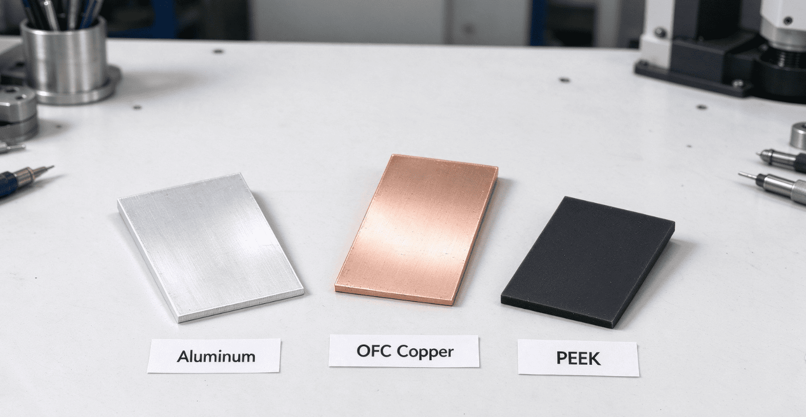
When designing custom vacuum hardware for wafer process chambers, three materials are frequently shortlisted: aluminum alloys, Oxygen-Free Copper (OFC / OFHC), and vacuum-grade PEEK. Each has unique outgassing behavior, plus tradeoffs on thermal conductivity, CNC machinability, plasma resistance and production cost. This article compares their outgassing performance and delivers practical material selection guidance for semiconductor vacuum components.
Material outgassing semiconductor vacuum: What Causes Outgassing in Aluminum, OFC Copper and PEEK
1. Aluminum (6061 / UHP Ultra-High Purity Aluminum)
Aluminum remains the dominant substrate material for semiconductor vacuum chamber bodies. It is widely selected for its light weight, balanced thermal conductivity and competitive raw material cost.
- Outgassing root cause: The native porous aluminum oxide surface layer readily traps water vapor. Anodized aluminum is NOT suitable for UHV applications, as thick hard anodizing absorbs massive moisture and continuously releases water under vacuum, drastically extending pump-down time. With proper chemical cleaning, electropolishing and controlled low-temperature bakeout, aluminum can achieve very low outgassing levels.
- Outgassing performance: Raw as-machined aluminum has moderate initial outgassing. After precision cleaning + low-temperature bake, outgassing drops significantly and can reach UHV-grade performance for many semiconductor process tools.
- Pros: High strength-to-weight ratio, excellent CNC machinability, good plasma corrosion resistance for most process gases, lower material cost compared with OFC copper.
- Limitations: Lower maximum bake temperature than stainless steel; not compatible with aggressive high-temperature bake cycles. Surface preparation is critical — poor surface finishing leads to severe water-related outgassing.
- Semiconductor vacuum use cases: Vacuum chamber frames, base plates, wafer fixture carriers, medium & low vacuum process modules, plasma-facing mechanical components.
2. OFC / OFHC Oxygen-Free Copper
Oxygen-Free Copper CNC machining for semiconductor produces high-purity copper with minimized oxygen content, engineered to eliminate hydrogen embrittlement and deliver ultra-low outgassing after controlled bakeout.
- Outgassing root cause: Bulk OFC copper contains extremely low trapped gas. Nearly all outgassing originates from surface-adsorbed water and carbon contaminants, instead of bulk material diffusion. Bakeout at 150–200°C effectively removes these surface adsorbed species.
- Outgassing performance: OFC copper is one of the best metal choices for ultra-low outgassing vacuum components after proper bakeout, ideal for thermal management parts inside vacuum systems.
- Pros: Outstanding thermal and electrical conductivity, minimal residual gas release post bakeout, high ductility. Commonly used for vacuum sealing gaskets and thermal straps.
- Limitations: Soft material, prone to creep under mechanical load at elevated temperatures. It oxidizes in air during high-temperature bake; oxide flakes may introduce particle contamination. Higher cost than aluminum, and poor plasma resistance.
- Semiconductor vacuum use cases: Thermal spreaders, cold-stage components, vacuum gaskets, RF feedthrough contacts, heat transfer hardware installed in non-plasma vacuum zones.
3. PEEK Polyetheretherketone (ESD Vacuum-Grade PEEK for Semiconductor)
PEEK CNC machining guide covers this leading high-performance engineering polymer approved for semiconductor high vacuum hardware. Engineers choose PEEK when metal materials fail to meet requirements for electrical isolation or matched thermal expansion.
- Outgassing root cause: Unlike metals, polymer outgassing comes from residual monomers from polymerization plus moisture trapped within the polymer matrix. ESD-grade PEEK uses a specialized formulation to reduce volatile outgassing for clean vacuum operation.
- Outgassing performance: Qualified vacuum-grade ESD PEEK can achieve ASTM E595 results of TML <0.3%, CVCM <0.05%. It works for many high-vacuum semiconductor applications, yet cannot match baked OFC copper for ultimate low outgassing in continuous UHV bake systems.
- Pros: Non-magnetic, low thermal conductivity, outstanding chemical resistance. Formulated ESD-safe grades prevent electrostatic discharge damage to sensitive wafers. Great electrical insulator for complex machined isolators and spacers.
- Limitations: Polymer outgassing rises sharply above its continuous service temperature (~250°C). It cannot withstand repeated high-temperature bake cycles required for UHV. Carbon ESD fillers may create particle risks without cleanroom-controlled CNC machining.
- Semiconductor vacuum use cases: Vacuum insulators, wafer contact spacers, standoffs, non-plasma internal fixtures, feedthrough insulating sleeves.
Material outgassing semiconductor vacuum: Side-by-Side Material Outgassing Comparison Table
| Material | Outgassing Characteristic | Key ASTM E595 | Thermal Conductivity | Bakeout Compatibility | Main Risk | Typical Semiconductor Vacuum Application |
|---|---|---|---|---|---|---|
| Aluminum (6061 / UHP, Electropolished) | Moderate initial outgassing; strong improvement after cleaning & low-temp bake; dominated by water vapor release | TML/CVCM not applicable for metals; performance fully surface-dependent | Medium-high | Limited maximum bake temperature; anodized aluminum forbidden for UHV | Moisture trapped in porous oxide layer | Chamber frames, baseplates, plasma-facing fixtures |
| OFC Copper | Ultra-low outgassing after bakeout; contamination limited to surface adsorbates | TML/CVCM not applicable for metals | Excellent | Bake at 150–200°C recommended | High-temperature oxidation, material creep | Thermal spreaders, vacuum gaskets, cold stages |
| Vacuum-Grade ESD PEEK | Low polymer outgassing; organic volatile release increases at high temperature | ESD grade: TML ~0.24%, CVCM <0.05% | Low | Not suitable for repeated high-temperature UHV bake | Accelerated organic outgassing over 250°C | ESD spacers, insulators, non-plasma internal fixtures |
How to Select Vacuum Materials Based on Your Semiconductor Process Requirements
Ultra-High Vacuum (UHV) / Contamination-Critical Processes (ALD, High-End PVD)
- Select OFC Copper for thermal transfer vacuum parts if oxidation risks can be managed.
- Use electropolished UHP Aluminum for chamber structural parts with strict surface treatment and constrained bake profiles.
- PEEK is not recommended for UHV systems requiring continuous high-temperature bake cycles.
High Vacuum + ESD Protection / Electrical Isolation
Vacuum-grade ESD PEEK is the primary option for non-plasma hardware without high-temperature bake requirements. Never substitute general-purpose industrial PEEK.
Cost-Sensitive Medium Vacuum Modules & Plasma-Facing Hardware
Aluminum alloy delivers the best balance of outgassing performance, CNC machinability and component cost.
Best Practices to Reduce Outgassing for All Vacuum Materials
Material choice is only half the battle. These critical processing steps minimize outgassing for aluminum, OFC copper and PEEK precision vacuum components:
- Process all vacuum hardware with precision cleanroom cleaning protocols; handle finished parts only with nitrile gloves after final cleaning.
- Fully remove residual machining oils, polishing compounds and adhesive residues.
- Specify proper surface finish: electropolishing for metal vacuum parts; avoid porous coatings and anodizing for UHV aluminum.
- Perform ASTM E595 or outgassing rate testing on material batches for new critical semiconductor projects.
- Minimize exposed surface area: reduce fine surface textures, hidden crevices and trapped-volume features that capture contaminants.
Conclusion
Outgassing performance is not an inherent fixed property of a raw material. It heavily depends on alloy purity, surface finishing, clean CNC machining quality and bakeout procedure.
- OFC Copper: Top low-outgassing metal option for vacuum thermal components; manage oxidation and creep risks.
- Aluminum: Versatile, cost-effective structural vacuum material; surface preparation defines final outgassing results.
- PEEK: Low-outgassing polymer solution for ESD isolation; subject to temperature and UHV bake limitations.
For semiconductor vacuum components, material selection must balance outgassing, thermal performance, plasma tolerance, particle control and manufacturing cost. If you need custom CNC machined semiconductor vacuum components with cleanroom processing and material certification, our engineering team supports prototype and volume production.
FAQ: Common Questions on Vacuum Material Outgassing for Semiconductors
Q: Is vacuum-grade PEEK low-outgassing enough for semiconductor vacuum systems?
A: Vacuum / ESD PEEK passes ASTM E595 with TML <1%, CVCM <0.1%. It is suitable for high-vacuum fixtures without bakeout or plasma exposure. It is not recommended for UHV systems with repeated high-temperature bake cycles.
Q: Can anodized aluminum be used inside semiconductor vacuum chambers?
A: Not recommended for high vacuum and UHV environments. Porous anodized oxide traps large volumes of water vapor, which continuously outgasses under vacuum, lengthening pump-down time and introducing wafer contamination risk.
Q: What is the difference between OFC and OFHC copper for UHV vacuum components?
A: OFHC (Oxygen-Free High Conductivity Copper) is the higher-purity grade of OFC copper. It features lower oxygen content, fewer inclusions and superior low-outgassing performance for semiconductor UHV hardware.
Q: How does bakeout reduce material outgassing in vacuum hardware?
A: Bakeout gently heats vacuum components under rough vacuum to drive off adsorbed water, carbon and volatile contaminants from material surfaces before chamber pump-down, greatly lowering steady-state outgassing rate.