

Surface Finishing Requirements for Semiconductor Vacuum CNC‑Machined Parts
Semiconductor vacuum systems are the core foundation of wafer etching, deposition, ion implantation and other chip‑manufacturing processes. Even tiny surface flaws, residual machining burrs, out‑gassing contaminants or improper surface texture on CNC‑machined vacuum components can destroy vacuum tightness, introduce particle contamination, and cause costly wafer‑batch failures.
For general industrial CNC parts, surface finishing mainly focuses on appearance, wear resistance or anti‑rust performance. For semiconductor vacuum equipment components, surface finishing is not an optional cosmetic step. It is a functional requirement directly related to vacuum level, particle control, out‑gassing rate and semiconductor production yield.
Many equipment designers and procurement engineers overlook finishing specifications at the early design phase. They only specify dimensional tolerance but skip surface roughness, cleaning standards and post‑processing rules. This will lead to parts that meet drawing dimension requirements but fail vacuum chamber testing. This article breaks down core surface finishing requirements, mainstream processes, material‑specific rules and common mistakes for semiconductor vacuum CNC‑machined parts.
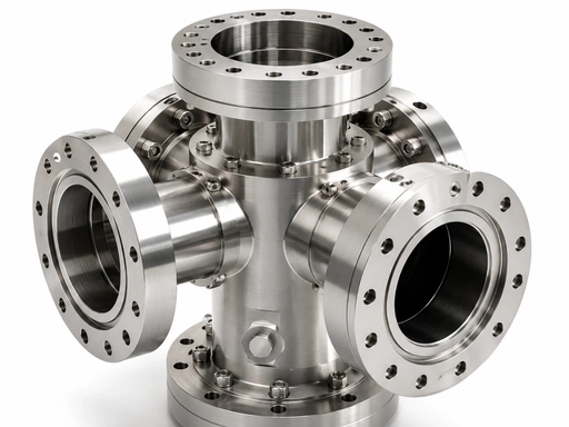
Why Surface Finishing Matters for Semiconductor Vacuum CNC‑Machined Components
In high‑vacuum and ultra‑high‑vacuum (UHV) semiconductor environments, every feature on the component surface impacts system performance. Three key risks come from poor surface finishing.
First, high out‑gassing. Rough, porous surfaces and residual cutting fluids trapped inside micro‑grooves will release gas molecules continuously under vacuum. Even qualified metal substrates will produce excessive out‑gassing if surface finishing is inadequate. Elevated out‑gassing lengthens pump‑down time and cannot reach target high‑vacuum pressure for wafer processing.
Second, particle generation. Sharp tool marks, burrs, loose surface grains and rough peaks will shed micro‑particles during equipment operation. Inside a semiconductor chamber, sub‑micron particles cause short circuits, pattern defects and wafer scrap. Clean‑room production sets strict particle limits, so vacuum parts must be finished to minimize particle shedding.
Third, corrosion risk and vacuum‑seal failure. Semiconductor processing generates corrosive process gases. Poor surface treatment creates crevices where corrosive media accumulate. For sealing surfaces such as flange grooves, uneven surface texture leads to imperfect gasket contact, resulting in vacuum leakage.
For these reasons, semiconductor vacuum CNC‑machined parts demand strict control over surface roughness, surface morphology, chemical purity and residual contamination.
Finishing processes must remove not only visual burrs, but also subsurface damage created during CNC turning and milling.
Core Surface‑Specification Metrics for Semiconductor Vacuum Parts
When drafting drawings and technical specifications for semiconductor vacuum components, three parameters must be clearly defined: surface roughness Ra, out‑gassing requirement, and clean‑room‑grade surface cleanliness.
Surface Roughness (Ra value)
- For general‑vacuum semiconductor parts, Ra 0.8 μm‑1.6 μm is common for non‑sealing inner‑chamber surfaces.
- For high‑vacuum inner surfaces: Ra ≤0.4 μm is widely specified.
- For UHV sealing flange contact surfaces: Ra ≤0.2 μm or lower is frequently required.
A low Ra value does not equal qualified vacuum performance. Some mechanical polishing can produce smooth surface while embedding abrasive particles. The finishing process itself matters more than only the Ra number.
Out‑gassing standard
Most semiconductor vacuum components follow ASTM E595 out‑gassing testing standard. Total mass loss (TML) and collected volatile condensable materials (CVCM) are two key indicators. Acceptable vacuum‑grade metal parts require low out‑gassing to avoid contaminating wafers. Organic residues from cutting oil, polishing paste must be fully removed.
Surface cleanliness
No residual CNC cutting fluid, no abrasive media residue, no fingerprints, no free iron contamination. Parts need solvent cleaning, ultrasonic cleaning and vacuum bake‑out as final finishing steps.
Main Surface‑Finishing Processes for Semiconductor Vacuum CNC‑Machined Parts
Different finishing technologies serve different vacuum‑level goals. CNC‑machined aluminum, stainless steel 304 / 316L are the most widely‑used substrate materials for semiconductor vacuum hardware.
1. Electropolishing (EP) — Top choice for UHV & high‑vacuum stainless‑steel vacuum parts
Electropolishing is the gold‑standard finishing process for stainless‑steel semiconductor vacuum components. It removes surface peaks uniformly by electrochemical dissolution, smoothing micro‑tool marks left by CNC milling.
Electropolishing brings multiple vacuum‑specific benefits:
- Produces a smooth, micro‑continuous passive chromium‑oxide surface layer
- Reduces real surface area, effectively lowering out‑gassing rate
- Removes embedded free iron from CNC machining, minimizing surface corrosion risk
- Eliminates micro‑crevices where particles and process by‑products can accumulate
For semiconductor vacuum flanges, chamber liners, beam‑line components made of 316L stainless steel, electropolishing is the default requirement. Important note: electropolishing removes material from part surfaces. CNC programmers must reserve proper material allowance for EP removal during machining, otherwise critical dimensions will go out‑of‑tolerance.
Electropolishing is less effective for aluminum alloys. Aluminum vacuum parts rarely adopt electropolishing as primary finishing.
2. Chemical passivation
Passivation is widely applied for stainless‑steel vacuum parts after CNC machining or mechanical polishing. The passivation process dissolves free iron embedded on part surfaces while building a stable chromium‑rich protective oxide film.
For semiconductor vacuum hardware, passivation shall follow ASTM A967 specification. It reduces surface corrosion risk and lowers particle‑shedding risk. Passivation does not change surface roughness greatly. It is usually a secondary process after polishing or electropolishing, not a standalone finishing solution for high‑vacuum requirements.
3. Abrasive blasting
Blasting creates a uniform matte surface texture. It can be used for non‑sealing outer surfaces of vacuum equipment housings.
Blasting is not recommended for inner high‑vacuum contact surfaces. Improper blasting will embed abrasive particles into metal surfaces. Embedded grit will fall off in vacuum conditions and generate harmful particles inside the chamber.
If blasting is required for semiconductor vacuum parts, operators must select vacuum‑grade blasting media, strictly control blasting parameters, and follow thorough multi‑step cleaning procedures to remove all residual media.
4. Mechanical polishing
Mechanical polishing can achieve low Ra value. However, mechanical polishing may press abrasives and polishing compound into metal subsurface layers. For semiconductor UHV environments, mechanical polishing alone is usually insufficient. It often needs follow‑up electropolishing and full cleaning to remove embedded contaminants.
5. Anodizing for aluminum vacuum components
Aluminum 6061 and 5052 are widely used for semiconductor vacuum structures because of low density and good machinability. Anodizing is the main finishing route for aluminum vacuum parts.
Hard‑coat anodizing produces a dense, inert aluminum‑oxide surface. It improves wear resistance and corrosion resistance. For vacuum service, thin‑film hard anodizing is preferred. Thick porous anodized layers trap gas and lead to high out‑gassing, which must be avoided for inner‑chamber vacuum surfaces.
Aluminum vacuum parts cannot use electropolishing as stainless steel does. Designers should specify suitable anodizing grades for aluminum vacuum hardware.
Material‑Based Finishing Guidelines for CNC‑Machined Semiconductor Vacuum Parts
Stainless Steel 316L (Most common UHV material)
- Inner high‑vacuum surface: Electropolishing is preferred, Ra ≤0.4 μm
- Sealing flange face: Electropolished, strict Ra control
- Outer non‑vacuum surface: Passivation or blasting allowed
- Post‑finishing: Ultrasonic cleaning, solvent degreasing, vacuum bake‑out
Stainless Steel 304
Suitable for moderate‑vacuum environments. 316L is preferred for critical semiconductor inner‑chamber components for better corrosion resistance. Finishing workflow is similar to 316L.
Aluminum 6061 / 5052
- Avoid electropolishing
- Inner vacuum surface: Controlled hard‑coat anodizing; avoid thick porous anodize
- Strictly remove all CNC coolant residue
- Bake‑out treatment is required to reduce out‑gassing
Common Mistakes in Semiconductor Vacuum‑Part Surface Finishing
Many finished CNC parts pass dimensional inspection yet fail vacuum‑system testing. These are frequent mistakes made by component suppliers:
- Treat surface finishing as cosmetic decoration. Engineers only mark dimension tolerance on drawings, without writing clear finishing, roughness and cleaning requirements. Suppliers apply standard general‑industry finishing and produce parts unsuitable for semiconductor vacuum.
- Wrong process selection. Applying blasting to inner UHV chamber surfaces, leading to embedded abrasive particles and particle contamination risk.
- Ignoring material removal caused by electropolishing. No stock allowance reserved in CNC programming. After EP processing, critical sizes shrink beyond tolerance range.
- Incomplete cleaning. Cutting fluid, polishing paste remain in tiny grooves, holes and thread roots. These residues cause high out‑gassing under vacuum. Cleaning and bake‑out are final finishing steps, not secondary optional work.
- Mix‑up of outer‑surface and inner‑vacuum‑surface requirements. Outer housing cosmetic finishing standards cannot be reused for inner chamber surfaces.
Complete Workflow for Semiconductor Vacuum CNC‑Machined Parts
A full qualified manufacturing workflow for semiconductor vacuum CNC components should follow this sequence:
- Precision CNC turning & milling, reserve proper stock allowance for subsequent surface finishing
- Manual or mechanical deburring: remove sharp burrs from holes, threads and edges
- Targeted surface finishing: electropolishing for stainless steel, hard‑coat anodizing for aluminum
- Passivation treatment (for stainless steel)
- Multi‑stage precision cleaning: solvent degreasing, ultrasonic cleaning, rinse with high‑purity deionized water
- Vacuum bake‑out to reduce out‑gassing
- Particle‑free packaging inside clean‑room environment
Conclusion
Surface finishing for semiconductor vacuum CNC‑machined parts is a functional engineering requirement rather than simple surface beautification. Different substrate materials and vacuum levels call for matching finishing solutions. Stainless‑steel UHV components mostly rely on electropolishing, while aluminum vacuum parts adopt qualified hard‑coat anodizing.
Surface roughness Ra value, out‑gassing performance and surface cleanliness should all be clearly specified on engineering drawings. Only controlling dimensional tolerance is not sufficient for semiconductor vacuum hardware. Improper finishing will cause vacuum leakage, particle pollution and wafer‑production losses.
When sourcing custom CNC‑machined semiconductor vacuum components, confirm whether your manufacturer has mature process experience for vacuum‑grade surface finishing, precision cleaning and bake‑out capability.
If you have custom vacuum component projects for semiconductor equipment, our team provides high‑precision CNC machining together with vacuum‑grade surface finishing according to your drawing specifications.
Feel free to send us your drawings for quotation and technical review.
Send Us Your Drawings For Quotation & Technical Review