Semiconductor crucibles are mission-critical carrier components for monocrystalline silicon growth, epitaxial deposition, and thin-film wafer processing. In modern fabs, high-precision CNC machining remains the only reliable manufacturing method to meet the extreme demands of ultra-clean, high-temperature, and vacuum environments.
This guide delivers 7 evidence-based facts that equipment buyers, process engineers, and supply chain managers need to know before sourcing custom semiconductor crucibles.
1. Core Applications of Custom Semiconductor Crucibles
When sourcing custom semiconductor crucibles, wafer fabs demand uncompromising precision, purity, and thermal stability.
2. Material Options for Custom Semiconductor Crucibles
Different wafer fabrication processes demand dedicated crucible materials. We support precision CNC processing across all major material categories:
| Material Category | Representative Grades | Key Advantages | Primary Applications |
|---|---|---|---|
| High-Purity Graphite | Isostatic Graphite | Withstands >3000°C, excellent thermal shock resistance, easy to machine | Czochralski silicon pulling (mainstream choice) |
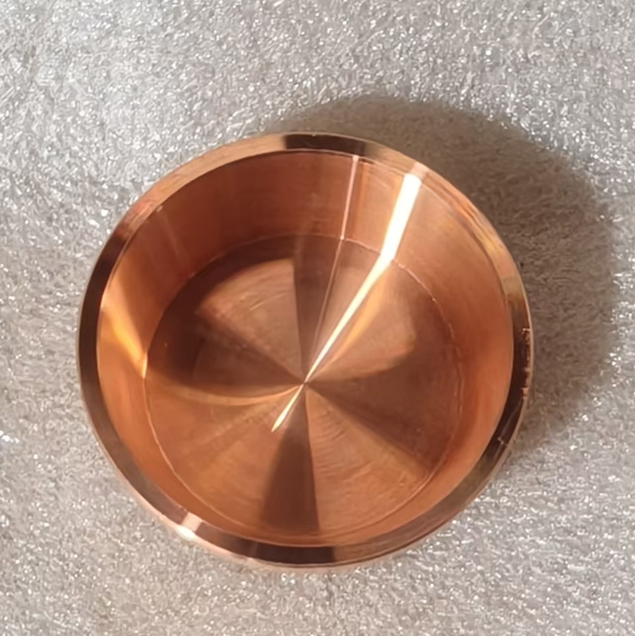
| Refractory Metals | Tantalum (Ta), Molybdenum (Mo) | Ultra-high vacuum compatibility, corrosion-resistant against molten semiconductors | MBE, MOCVD, and advanced epitaxy tools |
| Quartz / Fused Silica | Transparent SiO₂ | Low CTE, optically transparent for in-situ observation | R&D prototyping, small-batch pilot runs |
| Advanced Ceramics | Alumina (Al₂O₃), Silicon Carbide (SiC) | High hardness, low particle generation, chemically inert | Advanced packaging, micro-wafer transfer processes |
Compliance Commitment: All raw materials strictly follow SEMI International Standards (www.semi.org). We provide lot-specific purity test reports meeting Class 1 cleanroom entry requirements.